Etching Outerlayer Printed Circuit Boards
by Rudy Sedlak
RD Chemical Company
The Overview
The typical PCB (Printed Circuit Board) manufacturing operation today is building PCBs using a process described as pattern (electro)plating. In this process the outerlayer panel arrives at the etching operation with an “etch resist” of Tin or Tin/Lead protecting certain areas of the Copper foil, this defines the circuit pattern that will remain after etching. A cross section of a pattern (electro)plated PCB is shown in Figure 1. Figure 1: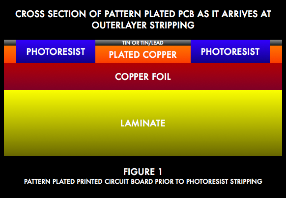
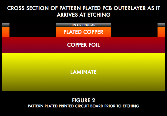
Figure 1 is a cross section of the PCB at the point of maximum build up, from this point in the process onwards, the process is subtractive, at least until the soldermask is applied.The next step after Figure 1. is to strip the photo-resist. This produces a board that should look like Figure 2.
After the photoresist is removed, the PCB is ready for etching.
Note that the copper on the PCB consists of two layers, but only one of the two layers is necessary to be removed in the outerlayer etching process to produce the final circuitry. This type of construction, pattern plated, is distinguished by the fact that electroplated copper is present only under the Tin (or Tin/Lead) etch resist.
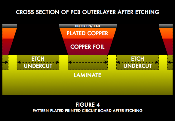
An alternate process produces a PCB where the plated copper covers the copper foil completely, with the photoresist defining only the Tin or Tin/Lead etch resist (see Figure 3.) Figure 3: There are other ways to configure the outerlayer manufacturing process, where the circuitry is protected, during etching, by photoresist, instead of a metal etch resist. In this case, the etching process more resembles the etching of innerlayers, which is covered in Innerlayer Process Fabrication, Etching. Tin or Tin/Lead is the most common etch resist used today. The use of Tin or Tin/Lead as an etch resist essentially mandates the use of ammoniacal etchant, because this is the only commonly used etchant chemistry that will not attack the Tin or Tin/Lead. When the term ammoniacal etchant is used here, it will refer to Ammonia/ Ammonium chloride etchant chemistry. There is also an Ammonia/Ammonium Sulfate etching chemistry that is commercially available. The Sulfate based etch chemistry is used to facilitate plating out of the copper from the etchant, thus allowing on-site recycling of the etchant. This sulfate based chemistry is not widely used, because it has a very slow etch rate, which would be expected in a non-Chloride etch chemistry.There has been some attempt at using Hydrogen Peroxide/Sulfuric Acid etches to etch outerlayers. This process has not been widely accepted commercially for various reasons, including economics and the issue of disposal of the spent etchant. Further the Hydrogen Peroxide/Sulfuric Acid etch process will not allow the use of a Tin (only) etch resist, and thus usually will require a Tin/Lead etch resist. This fact will make Sulfuric/Peroxide even less attractive, as the move to eliminate Lead from the printed circuit board manufacturing process becomes more widespread. The quality of etch can be minimally defined by the completeness of the removal of Copper which is not protected by the etch resist, and no more than that. However the definition of the quality of etch, in reality, also includes the straightness of trace edges, and the level of etch undercut. Etch undercut is a result of the fact that the etchant is not inherently directional, and will etch sideways as well as downwards. Etch undercut, (See Figure 4) is frequently discussed in terms of “etch factor”, which is defined as the amount of etch undercut divided by the amount of Copper that has been etched through (“X” in Figure 4). The PCB industry varies widely in its etch factor, and factors of from 1:1 to 1:5 are seen. Clearly, less undercut, or a lower number of the etch factor, is preferable. The etch factor, or the level of etch undercut, can be affected (it may be optimistic to say it can be controlled) by etch equipment configuration, and by the etch chemistry. Chemical agents called “banking agents” are present in the etch chemistry to minimize undercut. The exact nature of these additives is usually a closely guarded trade secret. Etch equipment configuration to minimize undercut will be discussed later. In many ways, the quality of etch is already defined before the PCB enters the etch chamber. The PCB manufacturing process is closely inter-connected, no one step stands alone. The result is that many of the problems that are diagnosed as “etch quality” originated in the resist stripper, or even previous to that in the process. The outerlayer etch is perhaps more prone to the deterioration of quality because of “upstream” problems in the process than most steps in the PCB manufacturing process. This is because of the fact that outerlayer etching is the last in a long series of steps, beginning with photoresist exposure, which define the outerlayer circuitry. Clearly, the more steps in a process, the more things can go wrong. This seems particularly the case in PCB manufacturing. The PCB, in theory, arrives at the etcher with a cross section pattern that looks like Figure 2.The optimum situation in the manufacturing of a pattern plated PCB is that the combined thickness of the Copper and Tin or Tin/Lead plating does not exceed the thickness of the Photoresist, and thus remains completely within the “well” defined by the walls of the photoresist. However, in the high pressure world of PCB manufacturing, it is common for the plating on certain areas of the panel to be excessive. So excessive in fact, that the plating extends over the top of the photoresist. When the plating is this much in excess, and it extends over the top of the photoresist “well”, it extends sideways also, and herein lies the real problem. This sideways extension creates a “lip” of Tin or Tin/Lead etch resist which extends over the top of the photoresist (see Figure 5). This lip of plated Tin, or Tin/Lead, etch resist makes complete removal of the photoresist during the resist stripping process prior to the etch, extremely difficult, leaving unstripped photoresist residues under the lip of metal etch resist. (See Figure 6). In the extreme case, residual photoresist can also cause a build up of scum in the etcher from the reaction of dissolved photoresist and Copper in the etcher, which can clog nozzles, pumps, and make it necessary to break down the etcher and clean it. Because of the powerful odor of Ammonia, this is one of the least liked jobs in the PCB industry, never mind the cost in production time. The ammoniacal etch is one of the more subtle and complex chemical processes in PCB manufacturing, yet paradoxically it is also one of the easier to run. The current technology, once set up properly, almost runs itself. However it is a process that does not adapt well to shutdowns, and is best run continuously. The process is heavily dependent on well set up (and maintained) equipment. As in all chemical etching, the use of a high pressure spray with properly chosen and configured nozzles is critical to obtaining high quality etching of the copper with straight side walls. There are many theories on the proper design and configuration of chemical etchers to obtain the straightest sidewalls, and many of them are conflicting. However all the theories agree that the basic concept is to get as much fresh etchant to the surface of the metal as fast as possible. Analysis of the chemical reactions of etching supports this outlook. In the case of the ammoniacal etch, assuming that all other parameters are in order, the etch rate is probably controlled by the availability of free Ammonia (NH3) in the etchant, and thus getting fresh etchant to the etch interface does two things, it sweeps away the just produced Cuprous ion, and supplies fresh Ammonia (NH3) to the etching reaction. Please refer to the Innerlayer Process Fabrication, Etching for a discussion of the chemistry of the ammoniacal etchant. Among the “ancient” lore of the PCB industry, and especially of the PCB suppliers industry, is the fact that the lower the Cuprous ion content of the ammoniacal etchant, the better (faster) it performs. And this is confirmed by experience. In fact, many ammoniacal etchants have Cuprous ion specific ligands (complexing agents), to effectively lower the available Cuprous ion, as part of their secret for high performance. Further, the Cuprous ion effect is not small. Etch rates can be more than doubled by reducing Cuprous from say 5000 ppm to under 50 PPM. Since Cuprous ion is being produced in large quantities by the etching reaction, it is difficult to keep the Cuprous ion concentration at near zero, and it is not made easier by the fact that the Cuprous ion is tightly bound in an Ammonia complex. The Cuprous ion is removed from the etchant by conversion to Cupric ion by reaction with atmospheric Oxygen. The Cuprous ion reacts with atmospheric Oxygen in the etch chamber, as the etchant is being sprayed. This is the functional reason why air is drawn through the etch chamber. However if too much air is drawn through the etcher, excessive Ammonia loss will result, and this will cause the pH of the etchant to drop, which also causes the etch rate to drop off, confirming the fact that Ammonia is the rate controlling agent. To counteract this, some users inject anhydrous Ammonia into the etch sump. This is typically done using a pH controller, which operates by signaling for the addition of Ammonia when the pH falls below a preset point. The allied field of chemical milling (also known as photo-chemical machining, or PCM) has produced some startling research into etcher configuration. And while the etchant used was Cupric Chloride, not Ammoniacal Copper etch, what was discovered should apply to the use of Ammoniacal etch in the PCB industry as well. The PCM industry typically etches foils that are 5-10 mils thick, and occasionally much thicker than that, consequently etch factor is even more critical than in the PCB industry. One set of research, from the PCM industry, which has never been published, produced startling results. The research was well funded, and thus the researchers were able to make profound changes in the design of the etcher, and check the effect of these changes on the etch factor. The optimum design was found to be one that used fan, as compared to cone nozzles, with the spray manifolds (the pipes that the nozzles are screwed into) turned, or angled, such that the sprays struck the work being etched as it entered the chamber at a 30° angle (see Figure 7). The last design factor that this research discovered is that there is an optimum spray pressure for each etch chemistry, and for certain etchants, this can be as high as 65 pounds/square inch (4+ Bar). For reference purposes, there are very few etching chambers in use today that can manage much above 30 pounds/square inch (2 Bar). It is a good rule of thumb that the higher the density (Specific Gravity, or Baume’) of an etchant, the higher the optimum spray pressure will be, but this is not the only factor. Another important factor is the relative mobility in solution of the etch rate controlling reagent. It is important to understand that the majority of etch quality problems are restricted to the top side of the panel being etched. This is because of the “puddling” effect of the etchant on the top of the printed circuit board. The top side of a printed circuit board panel builds up a thick puddle of etchant, that absorbs the energy of the sprays, and makes replenishment of the etchant at the surface of the metal a difficult, and relatively slow process. Puddling causes different etch patterns on the top versus the bottom of the PCB. Puddling is also the reason why the top side of the leading edge of panels get etched more thoroughly, or more commonly, over-etched. The mechanism for this is that the leading edge has not had time to develop a “puddle” of liquid on it when it is first introduced into the etch chamber, and thus etches quickly. The final part of the panel, however, will have a puddle on it as soon as it enters the etch chamber, and thus etches more slowly. The top versus bottom side difference in etch quality can be compensated for by adjustment of spray pressures on the top and bottom spray manifolds. There are some innovative designs now being proposed to compensate for the leading edge problem, that shut off the first few spray bars for a time after a panel enters the etch chamber. Perhaps the most critical factor in maintenance of an etcher is to insure that the spray nozzles are kept clean, and unclogged. Clogging can occur from the buildup of sludge in the etcher, or from bits of the PCB’s being etched which are knocked off by the force of the sprays. If the nozzles are not kept clean, the etching will be non-uniform from side to side, thus producing reject PCBs. Beyond the obvious maintenance of replacement of broken, and worn parts, including the replacement of nozzles, as they also wear, a key issue in etcher maintenance, is keeping the etcher free of sludge. Sludge can accumulate in many ways, and can even accumulate in an etcher where the chemistry is kept in balance. The sludge problem can get totally out of control if the chemistry is allowed to go out of balance. The magnitude of this problem is difficult to over emphasize. If the etchant does suddenly “sludge out”, it is usually a sign that the chemistry of the etchant was allowed to get out of balance, and it can be cleaned up with reasonably strong Hydrochloric Acid, or with etchant replenisher. Sludge can also be a buildup of photoresist, which, initially dissolves in the etchant, and then precipitates as a Copper salt. Photoresist sludge in the etcher is, of course, an indication that the photoresist stripping is inadequate. Poor photoresist stripping is symptomatic of marginal photoresist stripper combined with overplating. 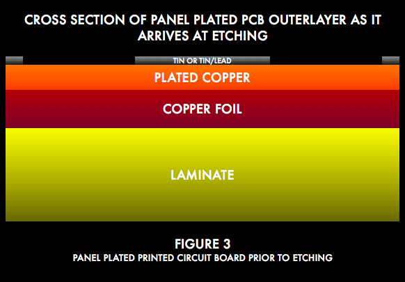
Etch Quality, and Pre-existing problems
Figure 5: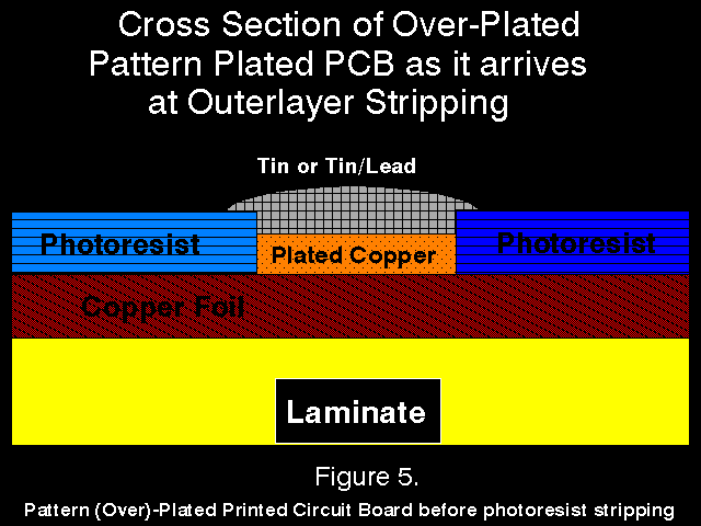
Figure 6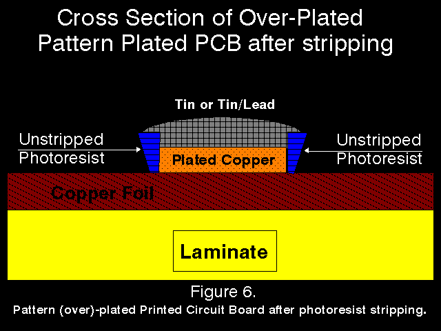 Residual, unstripped, photoresist can cause incomplete etching, which will be evidenced by a copper “foot” next to the trace after etching. The presence of this foot effectively narrows the space between the traces, and this can ultimately cause the PCB to be out of specification, and cause rejection. Rejection of the PCB at this point in the process is particularly expensive because most of the work (read “cost”) to produce the board has already gone into it at this point.
Equipment, Setup and Interaction with Etchant Chemistry
Figure 7: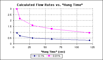
Figure 8: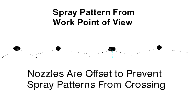
Top Side Versus Bottom Side Problems, and Leading Edge Issues
Etcher Equipment Maintenance
